

SPI 2 - A simple implementation
ARM processor
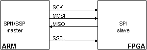
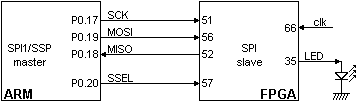
To get an opportunity to test our newly acquired SPI knowledge, we use a Saxo-L board. It has an ARM7 processor (LPC2138) and a Cyclone FPGA (EP1C3), connected by a SPI bus.
The ARM is used as a SPI master, while the FPGA is used as a SPI slave. The Saxo-L ARM processor has actually two SPI interfaces, one called SPI0, and a more advanced one called SPI1/SSP. They are both equally easy to use. We are using SPI1/SSP on Saxo-L, as it is pre-wired on the board.
SPI master - C ARM code
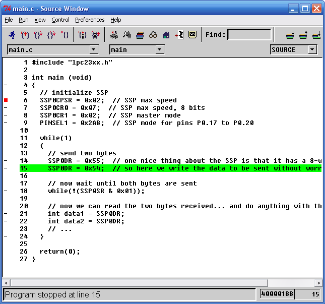
Using SSP is just a matter of initializing a few registers, and then writing/reading data to send/receive automatically.
void main(void)
{
  // initialize SSP
  SSP0CPSR = 0x02;  // SSP max speed
  SSP0CR0 = 0x07;  // SSP max speed, 8 bits
  SSP0CR1 = 0x02;  // SSP master mode
  PINSEL1 = 0x2A8;  // SSP mode for pins P0.17 to P0.20

  while(1)
  {
    // send two bytes
    SSP0DR = 0x55;  // one nice thing about the SSP is that it has a 8-words deep FIFO
    SSP0DR = 0x54;  // so here we write the data to be sent without worrying

    // now wait until both bytes are sent
    while(!(SSP0SR & 0x01));

    // now we can read the two bytes received... and do anything with them
    int data1 = SSP0DR;
    int data2 = SSP0DR;
    // ...
  }
}
SPI slave - HDL FPGA code
Now for the SPI slave in the FPGA.
Since the SPI bus is typically much slower than the FPGA operating clock speed, we choose to over-sample the SPI bus using the FPGA clock. That makes the slave code slightly more complicated, but has the advantage of having the SPI logic run in the FPGA clock domain, which will make things easier afterwards.
First the module declaration.
module SPI_slave(clk, SCK, MOSI, MISO, SSEL, LED);
input clk;

input SCK, SSEL, MOSI;
output MISO;

output LED;
Note that we have "clk" (the FPGA clock) and an LED output... a nice little debug tool. "clk" needs to be faster than the SPI bus. Saxo-L has a default clock of 24MHz, which works fine here.
We sample/synchronize the SPI signals (SCK, SSEL and MOSI) using the FPGA clock and shift registers.
// sync SCK to the FPGA clock using a 3-bit shift register
reg [2:0] SCKr;  always @(posedge clk) SCKr <= {SCKr[1:0], SCK};
wire SCK_risingedge = (SCKr[2:1]==2'b01);  // now we can detect SCK rising edges
wire SCK_fallingedge = (SCKr[2:1]==2'b10);  // and falling edges

// same thing for SSEL
reg [2:0] SSELr;  always @(posedge clk) SSELr <= {SSELr[1:0], SSEL};
wire SSEL_active = ~SSELr[1];  // SSEL is active low
wire SSEL_startmessage = (SSELr[2:1]==2'b10);  // message starts at falling edge
wire SSEL_endmessage = (SSELr[2:1]==2'b01);  // message stops at rising edge

// and for MOSI
reg [1:0] MOSIr;  always @(posedge clk) MOSIr <= {MOSIr[0], MOSI};
wire MOSI_data = MOSIr[1];
Now receiving data from the SPI bus is easy.
// we handle SPI in 8-bit format, so we need a 3 bits counter to count the bits as they come in
reg [2:0] bitcnt;

reg byte_received;  // high when a byte has been received
reg [7:0] byte_data_received;

always @(posedge clk)
begin
  if(~SSEL_active)
    bitcnt <= 3'b000;
  else
  if(SCK_risingedge)
  begin
    bitcnt <= bitcnt + 3'b001;

    // implement a shift-left register (since we receive the data MSB first)
    byte_data_received <= {byte_data_received[6:0], MOSI_data};
  end
end

always @(posedge clk) byte_received <= SSEL_active && SCK_risingedge && (bitcnt==3'b111);

// we use the LSB of the data received to control an LED
reg LED;
always @(posedge clk) if(byte_received) LED <= byte_data_received[0];
Finally the transmission part.
reg [7:0] byte_data_sent;

reg [7:0] cnt;
always @(posedge clk) if(SSEL_startmessage) cnt<=cnt+8'h1;  // count the messages

always @(posedge clk)
if(SSEL_active)
begin
  if(SSEL_startmessage)
    byte_data_sent <= cnt;  // first byte sent in a message is the message count
  else
  if(SCK_fallingedge)
  begin
    if(bitcnt==3'b000)
      byte_data_sent <= 8'h00;  // after that, we send 0s
    else
      byte_data_sent <= {byte_data_sent[6:0], 1'b0};
  end
end

assign MISO = byte_data_sent[7];  // send MSB first
// we assume that there is only one slave on the SPI bus
// so we don't bother with a tri-state buffer for MISO
// otherwise we would need to tri-state MISO when SSEL is inactive

endmodule
We have established communication between the ARM and the FPGA!
Running the code
As we step through the ARM code, we can see the LED changing state, and the data returned by the FPGA.
Now let's see if we can do useful things with SPI.