

FPGAs 2 - How do they work?
Logic-cells
FPGAs are built from one basic "logic-cell", duplicated hundreds or thousands of time. A logic-cell is basically a small lookup table ("LUT"), a D flip-flop and a 2-to-1 mux (to bypass the flip-flop if desired).
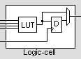
The LUT can implement any logic function. It has typically a few inputs (4 in the drawing above), so for example an AND gate with 3 inputs, whose result is then OR-ed with another input would fit in one 4-input LUT.
Interconnect
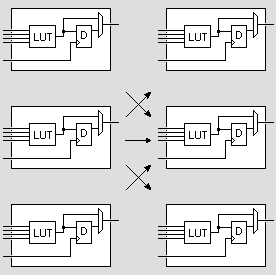
Each logic-cell can be connected to other logic-cells through interconnect resources (wires/muxes placed around the logic-cells). Each cell can do little, but with lots of them connected together, complex logic functions can be created.
IO-cells
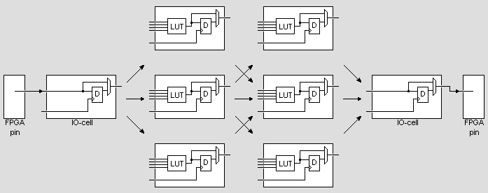
The interconnect wires also go to the boundary of the device where I/O cells are implemented and connected to the pins of the FPGAs.
Dedicated routing/carry chains
In addition to general-purpose interconnect resources, FPGAs have fast dedicated lines in between neighboring logic cells. The most common type of fast dedicated lines are "carry chains". Carry chains allow creating arithmetic functions (like counters and adders) efficiently (low logic usage & high operating speed). For more info, check this page.
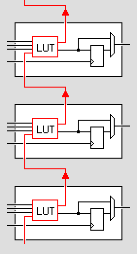
Older programmable technologies (PAL/CPLD) don't have carry chains and so are quickly limited when arithmetic operations are required.