

HDMI
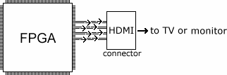
HDMI is a digital video interface, so is easy to drive from modern FPGAs.
Let's see how it works.
The connector
A standard HDMI connector has 19 pins. Out of the 19 pins, 8 are of particular interest as they form 4 TMDS differential pairs to transport the actual high-speed video info.
- TMDS clock+ and clock-
- TMDS data0+ and data0-
- TMDS data1+ and data1-
- TMDS data2+ and data2-
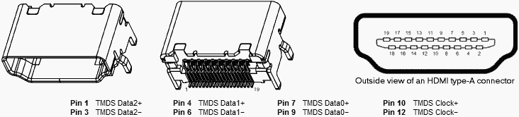
Our connection from an FPGA to an HDMI connector can hardly be simpler... we use 8 FPGA pins configured as 4 differential TMDS outputs.
Video signal
Let's create a 640x480 RGB 24bpp @ 60Hz video signal. That's 307200 pixels per frame, and since each pixel has 24 bits (8 bits for red, green and blue), at 60Hz, the HDMI link transports 0.44Gbps of "useful" data.
But video signals usually also have an "off-screen" area, which is used by the HDMI receiver (TV or monitor) for some housekeeping. Our 640x480 frame is actually sent as an 800x525 frame.
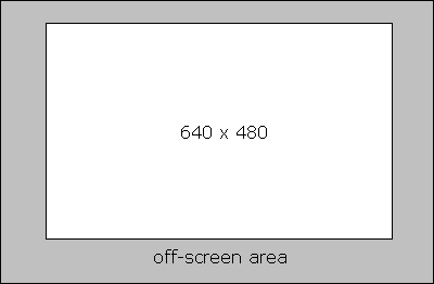
With that in mind, we need a 24.5MHz pixel clock to achieve 60 frames per seconds, but HDMI specifies a 25MHz minimum pixel clock, so that's we use (which gets us a 61Hz frame rate).
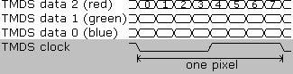
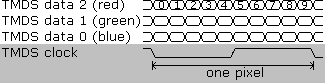
TMDS signals
The FPGA has 4 TMDS differential pairs to drive.
First, the TMDS clock is simply the pixel clock, so it runs at 25MHz.
The other 3 pairs transmit the red, green and blue 8bit signals, so we get something like that.
Things are in fact just a bit more complicated. HDMI requires that we scramble the data and add 2 bits per color lane, so we have 10 bits instead of 8 and the link ends up transporting 30 bits per pixel. The scrambling and extra bits are needed by the HDMI receiver to properly synchronize to and acquire each lane (check the DVI and HDMI specifications for all the details).
Source code
First a video generator. We use a couple of counters that go through an 800x525 pixel area...
reg [9:0] CounterX;  // counts from 0 to 799
always @(posedge pixclk) CounterX <= (CounterX==799) ? 0 : CounterX+1;

reg [9:0] CounterY;  // counts from 0 to 524
always @(posedge pixclk) if(CounterX==799) CounterY <= (CounterY==524) ? 0 : CounterY+1;
and create the h-sync and v-sync signals...
wire hSync = (CounterX>=656) && (CounterX<752);
wire vSync = (CounterY>=490) && (CounterY<492);
wire DrawArea = (CounterX<640) && (CounterY<480);
and generate some red, green and blue signals (8 bits each)...
wire [7:0] red = {CounterX[5:0] & {6{CounterY[4:3]==~CounterX[4:3]}}, 2'b00};
wire [7:0] green = CounterX[7:0] & {8{CounterY[6]}};
wire [7:0] blue = CounterY[7:0];
which are expanded to 10 bits each through three "TMDS_encoder" instances...
wire [9:0] TMDS_red, TMDS_green, TMDS_blue;
TMDS_encoder encode_R(.clk(pixclk), .VD(red  ), .TMDS(TMDS_red)  , .CD(2'b00)        , .VDE(DrawArea));
TMDS_encoder encode_G(.clk(pixclk), .VD(green), .TMDS(TMDS_green), .CD(2'b00)        , .VDE(DrawArea));
TMDS_encoder encode_B(.clk(pixclk), .VD(blue ), .TMDS(TMDS_blue) , .CD({vSync,hSync}), .VDE(DrawArea));
Now, we have three 10 bits values to be sent for every pixel clock period. We multiply the 25MHz clock by 10 to generate a 250MHz clock...
wire clk_TMDS, DCM_TMDS_CLKFX;
DCM_SP #(.CLKFX_MULTIPLY(10)) DCM_TMDS_inst(.CLKIN(pixclk), .CLKFX(DCM_TMDS_CLKFX), .RST(1'b0));

BUFG BUFG_TMDSp(.I(DCM_TMDS_CLKFX), .O(clk_TMDS));  // 250 MHz
and use three shift registers clocked at 250MHz...
reg [3:0] TMDS_mod10;  // modulus 10 counter
always @(posedge clk_TMDS) TMDS_mod10 <= (TMDS_mod10==9) ? 0 : TMDS_mod10+1;

reg TMDS_shift_load;
always @(posedge clk_TMDS) TMDS_shift_load <= (TMDS_mod10==9);

reg [9:0] TMDS_shift_red, TMDS_shift_green, TMDS_shift_blue;
always @(posedge clk_TMDS)
begin
    TMDS_shift_red   <= TMDS_shift_load ? TMDS_red   : TMDS_shift_red  [9:1];
    TMDS_shift_green <= TMDS_shift_load ? TMDS_green : TMDS_shift_green[9:1];
    TMDS_shift_blue  <= TMDS_shift_load ? TMDS_blue  : TMDS_shift_blue [9:1];
end
to send the TMDS data outside the FPGA.
OBUFDS OBUFDS_red  (.I(TMDS_shift_red  [0]), .O(TMDSp[2]), .OB(TMDSn[2]));
OBUFDS OBUFDS_green(.I(TMDS_shift_green[0]), .O(TMDSp[1]), .OB(TMDSn[1]));
OBUFDS OBUFDS_blue (.I(TMDS_shift_blue [0]), .O(TMDSp[0]), .OB(TMDSn[0]));
OBUFDS OBUFDS_clock(.I(pixclk), .O(TMDSp_clock), .OB(TMDSn_clock));
The complete source is available here.
Higher resolutions
With 640x480, we used 250MHz clocked serializers, but for higher resolutions, we need higher frequencies, which can quickly go above the ability of FPGAs. The workaround is to use some special FPGA IO features, like DDR outputs and IO serializers.
Another problem at higher frequencies is how to reliably transfer data from the pixel clock domain to the serializer domain. One possible technique is to use a shallow FIFO. Check the Xilinx XAPP460 (for Spartan-3A) and XAPP495 (for Spartan-6) application notes to get some ideas.
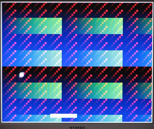
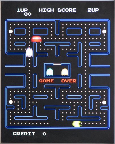
Screenshots
Here are a few shots made using a digital camera shooting an LCD monitor driven by a Pluto-IIx HDMI.
We have the pong game
and for fun, the classic PacMan arcade game (which was available from fpgaarcade.com before the site was re-designed - you can still get the original source code using the wayback machine).
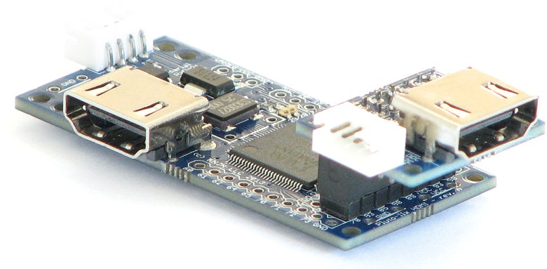
Here's a pic of our test board (Pluto-IIx HDMI loaded with an optional HDMI adapter - so we actually have two HDMI outputs to play with...).
Links
- A DVI and TMDS white paper from Silicon Image.
- An introduction to TMDS from BICSI.
- HDMI 1.3 demystified from audioquest.
- The DVI 1.0 specification (HDMI is based on DVI).
- The HDMI 1.3a specification (HDMI LA request).
- A list of video modes that monitors might support.
- A HDMI Display Output tutorial.
- The github hdl-util/hdmi and the Project F Display Controller HDMI projects.