

FPGAs 3 - Internal RAM
In addition to logic, all new FPGAs have dedicated blocks of static RAM distributed among and controlled by the logic elements.
Internal RAM operation
There are many parameters affecting RAM operation. The main parameter is the number of agents that can access the RAM simultaneously.
- "single-port" RAMs: only one agent can read/write the RAM.
- "dual-port" or "quad-port" RAMs: 2 or 4 agents can read/write. Great to get data across clock domains (each agent can use a different clock).
Here's a simplified drawing of a dual-port RAM.
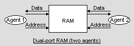
To figure out how many agents are available, count the number of separate address buses going to the RAM. Each agent has a dedicated address bus. Each agent has also a read and/or a write data bus.
Writing to the RAM is usually done synchronously. Reading is usually done synchronously but can sometimes be done asynchronously.
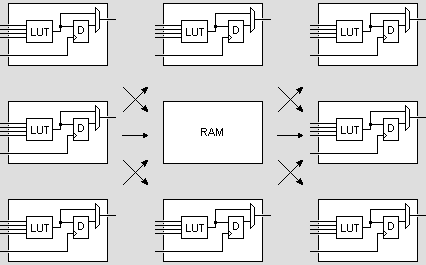
Blockram vs. Distributed RAM
Now there are two types of internal RAMs in an FPGA: blockrams and distributed RAMs. The size of the RAM needed usually determines which type is used.
- The big RAM blocks are blockrams, which are located in dedicated areas in the FPGA. Each FPGA has a limited number of these, and if you don't use them, you "loose" them (they cannot be used for anything but RAM).
- The small RAM blocks are either in smaller blockrams (Altera does that), or in "distributed RAM" (Xilinx does that). Distributed RAM allows using the FPGA logic-cells as tiny RAMs which provides a very flexible RAM distribution in an FPGA, but isn't efficient in term of area (a logic-cell can actually hold very few bits of RAM). Altera prefers building different size blockrams around the device (more area efficient, but less flexible). Which one is better for you depends on your FPGA application.