

PCI 2 - PCI Reads and Writes
Let's do some real PCI transactions now...
For WinXP/2K, GiveIO and UserPort are free generic drivers that open up the IO space.
The RAM is 32 bits x 16 locations. That's small enough to fit in IO space using "direct addressing" (the IO space is so crowded that indirect addressing is otherwise necessary).
We need to pick a free IO space in the host PC. Each 32-bit location takes 4 bytes addresses, so we require 4x16=64 contiguous free addresses. We chose 0x200-0x23F here but you may have to choose something else.
First the module declaration.
Then we keep track of what is happening on the bus through a "PCI_Transaction" register.
"PCI_Transaction" is asserted when any transaction is going on, either for us, or any other card on the bus.
Now a few more registers to be able to claim the transaction and remember if it's a read or a write
Let's claim the transaction.
Finally, the RAM itself is written or read, with the PCI_AD bus driven accordingly.
Now we can read and write the PCI card!
Some compilers don't have native support for these, so you may have to use inline assembler functions. Here are examples for Visual C++:
That works directly on Win98/Me. Be sure to have GiveIO or UserPort running on WinXP/2K.
One important thing: free spaces return 0xFFFFFFFF on reads.
But these registers add latencies to the design. The above code is simple enough that IO block registers are not required.
The code was tested using the Dragon board and Xilinx's ISE software.
It gives something like:
Clock frequency was largely met (103MHz against 33MHz).
Tsu was met by a large margin (5.556ns against 7ns) while Tco was barely met (10.932ns against 11ns) on the PCI_DEVSELn and PCI_TRDYn signals.
Tco would not have been met on the AD bus if the IO address had to be auto-incremented on burst reads. Since the address is static, and since (for read cycles only) the PCI bus requires a turnaround cycle after the address phase, the data has an extra clock cycle to get ready. Without it, the Tco was around 13ns, so above the maximum 11ns. But with the extra clock cycle, we actually meet the timing by a 28ns slack (=margin), which is very comfortable.
The only timing that was not met is the input hold-time (0nS), which was hopefully low enough (0.3nS for the worst violator). But Xilinx doesn't support a way to constraint the hold-time, maybe because using IO block registers guaranties "by design" (of the FPGA) a 0ns hold-time.
IO transactions
The easiest PCI space to work with is the IO space.- No virtualization from the CPU/OS (i.e. CPU address = hardware address)
- No driver necessary (true on Win98/Me, while on Win XP/2K, a driver is required but generic ones are provided below)
Finding a free space
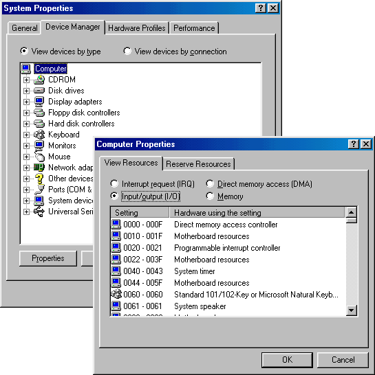
On Windows 98/Me, open the "Device Manager" (from "Control Panel"/System), then show Computer/Properties and check the "Input/Output (I/O)" panel.
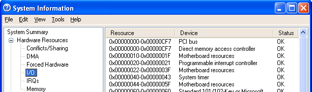
On Windows XP/2000, open the "System Information" program (Programs/Accessories/System Tools/System Information) and click on "I/O".
Device driver
The IO space is left unprotected on Win98/Me, so not driver is necessary there.For WinXP/2K, GiveIO and UserPort are free generic drivers that open up the IO space.
A RAM PCI card
Let's implement a small RAM in our PCI card.The RAM is 32 bits x 16 locations. That's small enough to fit in IO space using "direct addressing" (the IO space is so crowded that indirect addressing is otherwise necessary).
We need to pick a free IO space in the host PC. Each 32-bit location takes 4 bytes addresses, so we require 4x16=64 contiguous free addresses. We chose 0x200-0x23F here but you may have to choose something else.
First the module declaration.
|
module PCI_RAM( PCI_CLK, PCI_RSTn, PCI_FRAMEn, PCI_AD, PCI_CBE, PCI_IRDYn, PCI_TRDYn, PCI_DEVSELn ); input PCI_CLK, PCI_RSTn, PCI_FRAMEn, PCI_IRDYn; inout [31:0] PCI_AD; input [3:0] PCI_CBE; output PCI_TRDYn, PCI_DEVSELn; parameter IO_address = 32'h00000200; // 0x0200 to 0x23F parameter PCI_CBECD_IORead = 4'b0010; parameter PCI_CBECD_IOWrite = 4'b0011; |
Then we keep track of what is happening on the bus through a "PCI_Transaction" register.
"PCI_Transaction" is asserted when any transaction is going on, either for us, or any other card on the bus.
|
reg PCI_Transaction; wire PCI_TransactionStart = ~PCI_Transaction & ~PCI_FRAMEn; wire PCI_TransactionEnd = PCI_Transaction & PCI_FRAMEn & PCI_IRDYn; always @(posedge PCI_CLK or negedge PCI_RSTn) if(~PCI_RSTn) PCI_Transaction <= 0; else case(PCI_Transaction) 1'b0: PCI_Transaction <= PCI_TransactionStart; 1'b1: PCI_Transaction <= ~PCI_TransactionEnd; endcase // We respond only to IO reads/writes, 32-bit aligned wire PCI_Targeted = PCI_TransactionStart & (PCI_AD[31:6]==(IO_address>>6)) & (PCI_AD[1:0]==0) & ((PCI_CBE==PCI_CBECD_IORead) | (PCI_CBE==PCI_CBECD_IOWrite)); // When a transaction starts, the address is available for us to register // We just need a 4 bits address here reg [3:0] PCI_TransactionAddr; always @(posedge PCI_CLK) if(PCI_TransactionStart) PCI_TransactionAddr <= PCI_AD[5:2]; |
Now a few more registers to be able to claim the transaction and remember if it's a read or a write
|
wire PCI_LastDataTransfer = PCI_FRAMEn & ~PCI_IRDYn & ~PCI_TRDYn; // Is it a read or a write? reg PCI_Transaction_Read_nWrite; always @(posedge PCI_CLK or negedge PCI_RSTn) if(~PCI_RSTn) PCI_Transaction_Read_nWrite <= 0; else if(~PCI_Transaction & PCI_Targeted) PCI_Transaction_Read_nWrite <= ~PCI_CBE[0]; // Should we claim the transaction? reg PCI_DevSelOE; always @(posedge PCI_CLK or negedge PCI_RSTn) if(~PCI_RSTn) PCI_DevSelOE <= 0; else case(PCI_Transaction) 1'b0: PCI_DevSelOE <= PCI_Targeted; 1'b1: if(PCI_TransactionEnd) PCI_DevSelOE <= 1'b0; endcase // PCI_DEVSELn should be asserted up to the last data transfer reg PCI_DevSel; always @(posedge PCI_CLK or negedge PCI_RSTn) if(~PCI_RSTn) PCI_DevSel <= 0; else case(PCI_Transaction) 1'b0: PCI_DevSel <= PCI_Targeted; 1'b1: PCI_DevSel <= PCI_DevSel & ~PCI_LastDataTransfer; endcase |
Let's claim the transaction.
|
// PCI_TRDYn is asserted during the whole PCI_Transaction because we don't need wait-states // For read transaction, delay by one clock to allow for the turnaround-cycle reg PCI_TargetReady; always @(posedge PCI_CLK or negedge PCI_RSTn) if(~PCI_RSTn) PCI_TargetReady <= 0; else case(PCI_Transaction) 1'b0: PCI_TargetReady <= PCI_Targeted & PCI_CBE[0]; // active now on write, next cycle on reads 1'b1: PCI_TargetReady <= PCI_DevSel & ~PCI_LastDataTransfer; endcase // Claim the PCI_Transaction assign PCI_DEVSELn = PCI_DevSelOE ? ~PCI_DevSel : 1'bZ; assign PCI_TRDYn = PCI_DevSelOE ? ~PCI_TargetReady : 1'bZ; |
Finally, the RAM itself is written or read, with the PCI_AD bus driven accordingly.
|
wire PCI_DataTransferWrite = PCI_DevSel & ~PCI_Transaction_Read_nWrite & ~PCI_IRDYn & ~PCI_TRDYn; // Instantiate the RAM // We use Xilinx's synthesis here (XST), which supports automatic RAM recognition // The following code creates a distributed RAM, but a blockram could also be used (we have an extra clock cycle to get the data out) reg [31:0] RAM [15:0]; always @(posedge PCI_CLK) if(PCI_DataTransferWrite) RAM[PCI_TransactionAddr] <= PCI_AD; // Drive the AD bus on reads only, and allow for the turnaround cycle reg PCI_AD_OE; always @(posedge PCI_CLK or negedge PCI_RSTn) if(~PCI_RSTn) PCI_AD_OE <= 0; else PCI_AD_OE <= PCI_DevSel & PCI_Transaction_Read_nWrite & ~PCI_LastDataTransfer; // Now we can drive the PCI_AD bus assign PCI_AD = PCI_AD_OE ? RAM[PCI_TransactionAddr] : 32'hZZZZZZZZ; endmodule |
Now we can read and write the PCI card!
Design considerations
- The PCI_CBE byte enables are not used, so the software is supposed to issue only 32-bit transactions, aligned.
- You might be surprised to find that the PCI "PAR" signal (bus parity) is not used either.
While PAR generation is required for PCI compliance, its checking might not be because the PCs I have access to work fine without it... And since I cannot test it in real hardware, I omitted it. - The above code supports burst transfers, but current PC bridges don't seem to issue bursts (at least for the IO space).
x86 processors have support for burst IO instructions (REP INS/OUTS) but they end up being broken into individual transactions on the PCI bus.
Also I'm not sure if burst IO would require auto-incrementing the IO address, especially since the REP INS/OUTS instructions don't. But as not incrementing has happy consequences on timing (more details below), I kept the code this way.
Issue IO read/write transactions
On PC, you use the x8086 "IN" and "OUT" processor instructions to issue IO transactions.Some compilers don't have native support for these, so you may have to use inline assembler functions. Here are examples for Visual C++:
|
void WriteIO_DWORD(WORD addr, DWORD data) { __asm { mov dx, addr mov eax, data out dx, eax } } DWORD ReadIO_DWORD(WORD addr) { __asm { mov dx, addr in eax, dx } } |
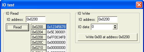
GUI PCI IO exerciser software
You can use this simple IOtest application to issue 32-bit IO reads and writes on a PC.That works directly on Win98/Me. Be sure to have GiveIO or UserPort running on WinXP/2K.
One important thing: free spaces return 0xFFFFFFFF on reads.
Timing considerations
Remember that PCI requires:- 7ns/0ns Tsu/Th (setup/hold) constraint on inputs
- 11ns Tco (clock-to-output) on outputs
But these registers add latencies to the design. The above code is simple enough that IO block registers are not required.
The code was tested using the Dragon board and Xilinx's ISE software.
It gives something like:
|
Timing summary: --------------- Timing errors: 0 Score: 0 Design statistics: Minimum period: 9.667ns (Maximum frequency: 103.445MHz) Minimum input required time before clock: 5.556ns Minimum output required time after clock: 10.932ns |
Clock frequency was largely met (103MHz against 33MHz).
Tsu was met by a large margin (5.556ns against 7ns) while Tco was barely met (10.932ns against 11ns) on the PCI_DEVSELn and PCI_TRDYn signals.
Tco would not have been met on the AD bus if the IO address had to be auto-incremented on burst reads. Since the address is static, and since (for read cycles only) the PCI bus requires a turnaround cycle after the address phase, the data has an extra clock cycle to get ready. Without it, the Tco was around 13ns, so above the maximum 11ns. But with the extra clock cycle, we actually meet the timing by a 28ns slack (=margin), which is very comfortable.
The only timing that was not met is the input hold-time (0nS), which was hopefully low enough (0.3nS for the worst violator). But Xilinx doesn't support a way to constraint the hold-time, maybe because using IO block registers guaranties "by design" (of the FPGA) a 0ns hold-time.