

PCI 3 - PCI logic analyzer
Now that we can issue read and write transactions on the bus, wouldn't it be fun to "see" how the transactions actually look like?
Here's a very simple transaction that was captured with Dragon.
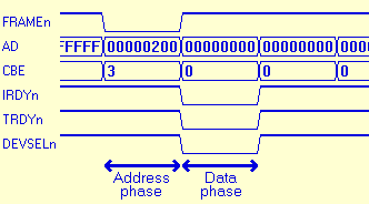
During the address phase, CBE is 0x3, which means "IO Write".
It's an IO Write, data 0x00000000, at address 0x0200.
The FPGA as a PCI logic analyzer
Being able to see the bus operation can be interesting to:- Get a better understanding of its operation.
- Check the bus latencies within and in-between transactions.
- Do post-mortem analysis (if you have functional problems in your PCI core).
Looking at the signals usually requires expensive equipment, like bus extenders and logic analyzers. That can be tricky because the PCI specification doesn't allow more than one IO load on each PCI signal (per PCI card of course). That's because the bus is sensitive to capacitive loads or wire stubs that would distort the high-speed signals.
But couldn't the FPGA act like a logic analyzer?
The FPGA is already connected to the bus, and has internal memories that can be used to capture the bus operation in real time. Dragon has also a USB interface that can be used to dump out the PCI captures without disturbing the PCI interface implementation, even if the PCI bus "dies".
The FPGA can also easily create complex triggers conditions that would outsmart most logic analyzers... what if you want to capture the 17th write after the second read at address 0x1234?
Capturing the PCI signals
We build a "state" (=synchronous) logic analyzer here.The signals captured are:
|
wire [47:0] dsbr = { PCI_AD, PCI_CBE, PCI_IRDYn, PCI_TRDYn, PCI_FRAMEn, PCI_DEVSELn, PCI_IDSEL, PCI_PAR, PCI_GNTn, PCI_LOCKn, PCI_PERRn, PCI_REQn, PCI_SERRn, PCI_STOPn}; |
Just 48 signals!
Nice, fit perfectly in 3 blockrams if we choose a depth of 256 clocks.
Implementation is easy: an 8-bit counter starts feeding the blockrams once a trigger condition is set, and another counter allows the USB to read the blockrams data. Logic was also added to allow some level of pre-trigger acquisition - details in the Dragon board files.
The blockram outputs are muxed out to the USB controller in this order
|
case(USB_readaddr[2:0]) 3'h0: USB_Data <= bro[ 7: 0]; 3'h1: USB_Data <= bro[15: 8]; 3'h2: USB_Data <= bro[23:16]; 3'h3: USB_Data <= bro[31:24]; 3'h4: USB_Data <= bro[39:32]; 3'h5: USB_Data <= bro[47:40]; 3'h6: USB_Data <= 8'h01; // padding, added for ease of implementation 3'h7: USB_Data <= 8'h02; // padding, added for ease of implementation endcase |
and finally, with a USB bulk read command, the data is acquired and saved into a ".pciacq" file for further analysis.
PCI bus viewer
The software used to view the ".pciacq" file can be downloaded here.A sample ".pciacq" file is included, which is the result capture of this list of transactions:
|
ReadIO_DWORD( 0x200 ); ReadIO_DWORD( 0x204 ); ReadIO_DWORD( 0x208 ); ReadIO_DWORD( 0x210 ); WriteIO_DWORD( 0x204, 0x12345678 ); WriteIO_DWORD( 0x208, 0x87654321 ); WriteIO_DWORD( 0x210, 0xDEADBEEF ); ReadIO_DWORD( 0x200 ); ReadIO_DWORD( 0x204 ); ReadIO_DWORD( 0x208 ); ReadIO_DWORD( 0x210 ); |
The software looks like:
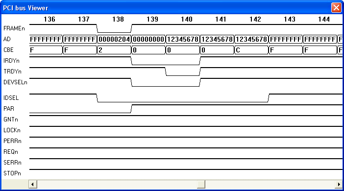
One interesting thing: during a read turnaround-cycle, the AD bus shows the data of the previous read... see cycle 151 for example... no idea why.
More PCI bus captures
If we issue an IO write transaction that is not claimed by anybody, the bridge used here retries 12 times!See this WriteNotClaimed.pciacq file (the first IO Write is claimed, the subsequent one is not and gets retried many times).
To view it, just un-zip and replace the original ".pciacq" file.
See also this ReadNotClaimed.pciacq file.