

Digital oscilloscope 1 - first design
Here's what is built here:
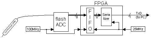
The FPGA receives two clocks:
Then, the FIFO content is read back, serialized and sent on a serial port at a much slower speed (115200 baud). Finally we connect the serial output to a PC that receives each byte and displays a signal trace.
For this first attempt, there is no trace triggering mechanism. The ADC storage starts at random intervals so the trace will jump left and right, but that's fine for now.
The serial communication used here works at 115200 bauds, so roughly 10KBytes/s. 1024 samples take about 100ms to transmit. During that time, the oscilloscope is "blind", because we discard the data coming from the ADC. So it is blind 99.99% of the time. That's typical of this type of architecture.
That can be partially compensated when we add a trigger mechanism later, because while the trigger is armed, it works at full ADC speed and can stay armed as long as it takes for the trigger condition to happen. More on that later.
Now "data_flash_reg" is fully internal to the FPGA and can be fed to the FPGA FIFO.
The FIFO uses synchronous static RAM blocks available inside the FPGA. Each storage block can store typically 512x8bit. So the FIFO uses 2 blocks.
The FIFO logic itself is created by using the FPGA vendor "function builder". Xilinx calls it "coregen" while Altera "Megafunctions wizard". Here let's use Altera's Quartus to create this file.
So now, using the FIFO is just a connectivity issue.
Using a FIFO is nice because it takes care of the different clocks. We connected the write side of the FIFO to the "clk_flash" (100MHz), and the read side of the FIFO to "clk" (25MHz).
The FIFO provides the full and empty signals for each clock domain. For example, "wrempty" is an empty signal that can be used in the write clock domain ("clk_flash"), and "rdempty" can be used in the read clock domain ("clk").
Using the FIFO is simple: Writing to it is just a matter of asserting the "wrreq" signal (and providing the data to the ".data" port), while reading from it a matter of asserting "rdreq" (and the data comes on the ".q" port).
We stop only when it gets full. And then the process starts again... we wait until it is empty... feed it until it is full... stop.
We use the async_transmitter module to serialize the data and transmit it to a pin called "TxD".
The FPGA receives two clocks:
- A slow "system" clock, fixed at 25MHz.
- An ADC sampling clock (something faster, let's say 100MHz), that is connected to both the ADC and the FPGA.
Then, the FIFO content is read back, serialized and sent on a serial port at a much slower speed (115200 baud). Finally we connect the serial output to a PC that receives each byte and displays a signal trace.
For this first attempt, there is no trace triggering mechanism. The ADC storage starts at random intervals so the trace will jump left and right, but that's fine for now.
Design considerations
At 100MHz, the FIFO fills up in about 10us. That's pretty fast. Once full, we have to stop feeding it. What is stored needs to be completely sent to the PC before we can start feeding the FIFO again.The serial communication used here works at 115200 bauds, so roughly 10KBytes/s. 1024 samples take about 100ms to transmit. During that time, the oscilloscope is "blind", because we discard the data coming from the ADC. So it is blind 99.99% of the time. That's typical of this type of architecture.
That can be partially compensated when we add a trigger mechanism later, because while the trigger is armed, it works at full ADC speed and can stay armed as long as it takes for the trigger condition to happen. More on that later.
Register the inputs
The ADC output data bus is connected to the FPGA using 8 pins that we call "data_flash[7:0]". These come at speed of up to 100MHz. Since this is fast, it is best to "register" them right when they come in the FPGA.|
reg [7:0] data_flash_reg; always @(posedge clk_flash) data_flash_reg <= data_flash; |
Now "data_flash_reg" is fully internal to the FPGA and can be fed to the FPGA FIFO.
The FIFO
The FIFO is 1024 words deep x 8-bit wide. Since we receive 8 bits per clock from the ADC, we can store 1024 ADC samples. At 100MHz, it takes about 10us to fill up the FIFO.The FIFO uses synchronous static RAM blocks available inside the FPGA. Each storage block can store typically 512x8bit. So the FIFO uses 2 blocks.
The FIFO logic itself is created by using the FPGA vendor "function builder". Xilinx calls it "coregen" while Altera "Megafunctions wizard". Here let's use Altera's Quartus to create this file.
So now, using the FIFO is just a connectivity issue.
| fifo myfifo(.data(data_flash_reg), .wrreq(wrreq), .wrclk(clk_flash), .wrfull(wrfull), .wrempty(wrempty), .q(q_fifo), .rdreq(rdreq), .rdclk(clk), .rdempty(rdempty)); |
Using a FIFO is nice because it takes care of the different clocks. We connected the write side of the FIFO to the "clk_flash" (100MHz), and the read side of the FIFO to "clk" (25MHz).
The FIFO provides the full and empty signals for each clock domain. For example, "wrempty" is an empty signal that can be used in the write clock domain ("clk_flash"), and "rdempty" can be used in the read clock domain ("clk").
Using the FIFO is simple: Writing to it is just a matter of asserting the "wrreq" signal (and providing the data to the ".data" port), while reading from it a matter of asserting "rdreq" (and the data comes on the ".q" port).
Writing to the FIFO
To start writing to the FIFO, we wait until it is empty. Of course, at power-up (after the FPGA is configured), that is true.We stop only when it gets full. And then the process starts again... we wait until it is empty... feed it until it is full... stop.
|
reg fillfifo; always @(posedge clk_flash) if(~fillfifo) fillfifo <= wrempty; // start when empty else fillfifo <= ~wrfull; // stop when full assign wrreq = fillfifo; |
Reading to the FIFO
We read from the FIFO as long as it is not empty. Each byte read is send to a serial output.|
wire TxD_start = ~TxD_busy & ~rdempty; assign rdreq = TxD_start; async_transmitter async_txd(.clk(clk), .TxD(TxD), .TxD_start(TxD_start), .TxD_busy(TxD_busy), .TxD_data(q_fifo)); |
We use the async_transmitter module to serialize the data and transmit it to a pin called "TxD".
Complete design
Our first working oscilloscope design, isn't that nice?|
module oscillo(clk, TxD, clk_flash, data_flash); input clk; output TxD; input clk_flash; input [7:0] data_flash; reg [7:0] data_flash_reg; always @(posedge clk_flash) data_flash_reg <= data_flash; wire [7:0] q_fifo; fifo myfifo(.data(data_flash_reg), .wrreq(wrreq), .wrclk(clk_flash), .wrfull(wrfull), .wrempty(wrempty), .q(q_fifo), .rdreq(rdreq), .rdclk(clk), .rdempty(rdempty)); // The flash ADC side starts filling the fifo only when it is completely empty, // and stops when it is full, and then waits until it is completely empty again reg fillfifo; always @(posedge clk_flash) if(~fillfifo) fillfifo <= wrempty; // start when empty else fillfifo <= ~wrfull; // stop when full assign wrreq = fillfifo; // the manager side sends when the fifo is not empty wire TxD_busy; wire TxD_start = ~TxD_busy & ~rdempty; assign rdreq = TxD_start; async_transmitter async_txd(.clk(clk), .TxD(TxD), .TxD_start(TxD_start), .TxD_busy(TxD_busy), .TxD_data(q_fifo)); endmodule |