

JTAG 1 - What is JTAG?
JTAG is an IEEE standard (1149.1) developed in the 1980s to solve electronic boards manufacturing issues. Nowadays it finds more use as programming, debug and probing port.
But first, let's see JTAG's original use, boundary testing.
Boundary testing
Here's a simple electronic board (also called "PCB" for "printed circuit board") with two ICs ("integrated circuits"), a CPU and an FPGA. A typical board may have many more ICs.
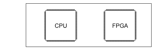
ICs can have lots of pins.
So of course, ICs are connected together with lots of connections (PCB traces).
We show just four here.
But you can easily have a few thousands on a PCB.
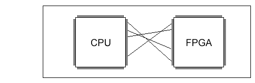
Now if you build a thousand boards, each with a few a thousand connections, you inevitably have a few bad boards.
How do you test all these boards? You have to make sure that all these connections are fine.
You can't just test all these connections by hand. So JTAG was created.
JTAG can take control (or hijack) the pins of all the ICs. On the picture, maybe JTAG is going to make all the CPU pins outputs, and all the FPGA pins inputs. Then by sending some data from the CPU pins, and reading the values from the FPGA pins, JTAG can make sure that the board connections are fine.
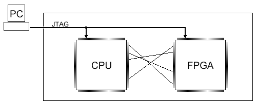
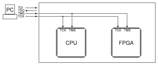
Now JTAG really consists of four logic signal, named TDI, TDO, TMS and TCK.
From the PC's point of view, that's three outputs, and one input.
These four signals need to be wired in a particular way.
First TMS and TCK are wired in parallel to all JTAG ICs.
Then TDI and TDO and connected to form a chain.
In JTAG terminology, you often hear the term "JTAG-chain", that's where it comes from.
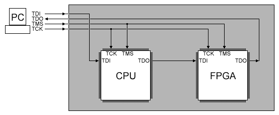
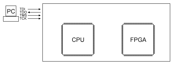
As you can see, each JTAG compliant IC has four pins used for JTAG (three inputs, and one output). A fifth pin named TRST is optional (JTAG reset). The JTAG pins are usually dedicated (not shared for other purposes).
All big ICs use boundary testing using JTAG - boundary testing is the original reason JTAG was created. Nowadays JTAG use has been extended to allow things like configuring FPGAs and then use JTAG inside the FPGA core for debug purpose.