

I2C slave (method 1)
There are two ways to create an I2C slave in an FPGA or CPLD.
That's the "black magic" part of this design...
The complete code is available here.
This code has two drawbacks:
Otherwise, use an external clock to oversample SDA and SCL (method 2). This way, glitches can be filtered out using digital filters, and the start and stop condition detected easily (at the price of a more complex design).
- Using directly the SCL line as a clock signal inside your FPGA/CPLD
- Using a fast clock to oversample the SDA and SCL signals
The first method allows creating a compact design. But it is not as reliable as the second method.
Example of I2C slave: IO extender, using method 1 (SCL as a clock in the FPGA/CPLD)
Here's a view of our IO extender.
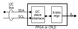
The I2C slave module is connected to a small 8-bit memory that can be read and written from the I2C bus. The 8 bits are also exported outside the FPGA/CPLD. That creates an I2C IO extender.
First the module declaration.module I2CslaveWith8bitsIO(SDA, SCL, IOout); inout SDA; input SCL; output [7:0] IOout;Then the 7-bit address that we want for our I2C slave.
parameter I2C_ADR = 7'h27;Then the start and stop conditions detection logic.
That's the "black magic" part of this design...
// We use two wires with a combinatorial loop to detect the start and stop conditions
//  ... making sure these two wires don't get optimized away
wire SDA_shadow    /* synthesis keep = 1 */;
wire start_or_stop /* synthesis keep = 1 */;
assign SDA_shadow = (~SCL | start_or_stop) ? SDA : SDA_shadow;
assign start_or_stop = ~SCL ? 1'b0 : (SDA ^ SDA_shadow);

reg incycle;
always @(negedge SCL or posedge start_or_stop)
    if(start_or_stop) incycle <= 1'b0; else if(~SDA) incycle <= 1'b1;
Now we are ready to count the I2C bits coming in
reg [3:0] bitcnt;  // counts the I2C bits from 7 downto 0, plus an ACK bit
wire bit_DATA = ~bitcnt[3];  // the DATA bits are the first 8 bits sent
wire bit_ACK = bitcnt[3];  // the ACK bit is the 9th bit sent
reg data_phase;

always @(negedge SCL or negedge incycle)
if(~incycle)
begin
    bitcnt <= 4'h7;  // the bit 7 is received first
    data_phase <= 0;
end
else
begin
    if(bit_ACK)
    begin
    	bitcnt <= 4'h7;
    	data_phase <= 1;
    end
    else
    	bitcnt <= bitcnt - 4'h1;
end
and detect if the I2C address matches our own
wire adr_phase = ~data_phase;
reg adr_match, op_read, got_ACK;
// sample SDA on posedge since the I2C spec specifies as low as 0µs hold-time on negedge
reg SDAr;  always @(posedge SCL) SDAr<=SDA;
reg [7:0] mem;
wire op_write = ~op_read;

always @(negedge SCL or negedge incycle)
if(~incycle)
begin
    got_ACK <= 0;
    adr_match <= 1;
    op_read <= 0;
end
else
begin
    if(adr_phase & bitcnt==7 & SDAr!=I2C_ADR[6]) adr_match<=0;
    if(adr_phase & bitcnt==6 & SDAr!=I2C_ADR[5]) adr_match<=0;
    if(adr_phase & bitcnt==5 & SDAr!=I2C_ADR[4]) adr_match<=0;
    if(adr_phase & bitcnt==4 & SDAr!=I2C_ADR[3]) adr_match<=0;
    if(adr_phase & bitcnt==3 & SDAr!=I2C_ADR[2]) adr_match<=0;
    if(adr_phase & bitcnt==2 & SDAr!=I2C_ADR[1]) adr_match<=0;
    if(adr_phase & bitcnt==1 & SDAr!=I2C_ADR[0]) adr_match<=0;
    if(adr_phase & bitcnt==0) op_read <= SDAr;
    // we monitor the ACK to be able to free the bus when the master doesn't ACK during a read operation
    if(bit_ACK) got_ACK <= ~SDAr;

    if(adr_match & bit_DATA & data_phase & op_write) mem[bitcnt] <= SDAr;  // memory write
end
and drive the SDA line when necessary.
wire mem_bit_low = ~mem[bitcnt[2:0]];
wire SDA_assert_low = adr_match & bit_DATA & data_phase & op_read & mem_bit_low & got_ACK;
wire SDA_assert_ACK = adr_match & bit_ACK & (adr_phase | op_write);
wire SDA_low = SDA_assert_low | SDA_assert_ACK;
assign SDA = SDA_low ? 1'b0 : 1'bz;

assign IOout = mem;
endmodule
What's the result?
The code has been tested in multiple devices (Xilinx FPGA, Altera FPGA/CPLD), with an hard-macro I2C master (Dragon board).The complete code is available here.
This code has two drawbacks:
- The SCL signal is used as a clock in the FPGA/CPLD. The use of a Schmitt trigger on the SCL input pin is strongly recommended to avoid erratic behavior (without Schmitt trigger, any noise or ringing on the SCL line may introduce extra clock cycles, which would break the functionality).
- The start and stop conditions detection logic uses a combinatorial feedback loop, which is not a recommended practice. Same thing on the "incycle" signal that is used as asynchronous reset by the rest of the logic. These are the price to pay to avoid using an oversampling clock.
Otherwise, use an external clock to oversample SDA and SCL (method 2). This way, glitches can be filtered out using digital filters, and the start and stop condition detected easily (at the price of a more complex design).