

SDRAM 1 - From static to dynamic
Static memories
Let's assume we want to connect a 16Mb memory to an FPGA.
16Mb means the memory holds 16 million bits (or 16,777,216 to be exact). Now the bits are rarely addressed individually, but usually in packets of 8 or 16 (we call that words). So if our 16Mb memory is organized as 1M words of 16bit, we need a 20bit address bus and a 16bit data bus, plus some write-enable and read-enable signals.
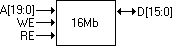
Real memories would also have a CS (chip-select), and if the memory is synchronous, a clock (these are omitted from the picture for clarity).
Now if this memory was a blockram (inside an FPGA), it would look different (assuming such big 16Mb blockram existed... typical blockrams are much smaller).
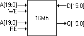
As you can see, it's still one block of memory but there are two address buses. That's because blockrams in modern FPGAs are dual-ported... which means two agents can access the memory at the same time. Usually one agent writes to the memory while the another reads. So the memory has independent address and data buses for each agent. The picture above shows the first (writing) agent on top and the second (reading) at the bottom. More advanced blockrams allow each agent to both read and write, but the architecture shown above is the most commonly used. Also blockrams are usually used synchronously, so each agent has to provide a clock (not shown on the picture).
The memories shown so far are static, which mean they hold their content simply by having power applied to them. A static memory can be seen as a long linear array of words (you simply provide an address and have access to the matching data... no complication). The trade-off is that the cost per bit is much higher than with...
Dynamic memories
We are going to work with an SDRAM, which is a dynamic memory (the "D" in SDRAM). And in a dynamic memory, the memory is not seen as a long linear array of words, but instead is organized as a matrix (row/column) of words.
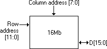
The picture above shows 12 bits for the row and 8 bits for the column, for a total of 20 address bits as before... easy.
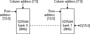
There is one complication: to improve performance, the memory is split in equal chunks called "banks". That's because some dynamic memory operations are slow, so having banks allows working with one bank while waiting for another.
So if our 16Mb SDRAM has 2 banks, each bank holds 8Mb.
When the SDRAM is accessed, the FPGA has to select the bank (1 bit), the row (only 11 bits now) and the column (8 bits), for a total of 20 bits. But that's a two steps process: first the row+bank, then the column:
- The FPGA chooses a bank and activates one of its row. Then it waits a few clocks (for the row to be ready).
- Now the row is active and the FPGA can access (read and/or write) any data it wants in the row simply by providing a column address.
- Once the FPGA is done working with the row, it has to close the row before opening a new one.
For the best performance, the user (=FPGA) wants to avoid opening and closing rows too much, but instead do as much work in a row as possible before closing it, and interleave operations in different banks so that no clock cycle is wasted. Most SDRAMs actually have 4 or 8 banks, and each bank is independent, so can have its own row active.
SDRAM pins
If we look at the pins of an SDRAM, there are a few newcomers.
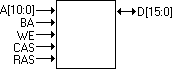
The address and data buses are still there, but the address bus has only 11 bits (it is used to provide the row to open, and then the column addresses). The BA pin specifies the bank (since we have only 2 banks in our example, we need only one pin). The WE, CAS and RAS are used together as command pins, so we can send 8 different commands to the SDRAM (commands include "open row", "read", "write", and "close row"). A few other pins are used (but not shown on the picture), like a clock, chip-select, byte-enable...
Note that in dynamic memory parlance, "open row" is called activate, and "close row" is called precharge.
Refresh
SDRAMs are dynamic memories: their content needs to be refreshed periodically because each memory bit value (0 or 1) is held in a tiny capacitor whose charge decays with time. But the decay rate is low enough that as long as it is read and re-written back periodically ("refreshed"), the manufacturer guarantees that no data will be lost.
Two refresh mechanisms are available.
- The FPGA sends the "auto-refresh" command to the SDRAM.
Just make sure it is done periodically (the SDRAM datasheet tells you the minimum refresh frequency). - The FPGA accesses each row "often enough".
Opening a row causes sense amplifiers in the SDRAM to get a copy of all the capacitor charges of that row. Then when the row is closed, the values sensed earlier are copied back into the capacitors, refreshing the data in the process.
Why a memory controller?
Dynamic memories are more complicated to drive than static ones... we have rows and columns and banks and refresh cycles to take care of. But SDRAMs are compelling thanks to their high-speed and low cost per bit.
So what we need is a way to access an SDRAM, but with the ease of use of a static memory. That's why memory controllers are created. They act as translation layers: on one side, they provide the user an easy to use memory interface, and then do the dirty work to drive the real SDRAM signals.