SDRAM 2 - A simple controller
Our SDRAM controller has the following features:
- Easy to use: make an SDRAM look like a static memory (or as close as possible anyway).
- Fast: SDRAM is used in burst mode if you provide continuous addresses.
- Simple: no scheduling, only one bank is active at a time.
- Powerful: SDRAM appears as a simple dual-port memory (i.e. with one writing agent and one reading agent).
The most uncommon feature of our controller might be the last one. SDRAMs are a single-port memories, but FPGAs greatly benefit from having access to dual-port memories (like blockrams), so we felt it was a nice feature to have.
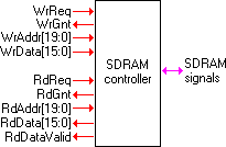
Controller signals
Here's a simplistic view of our SDRAM controller.
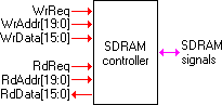
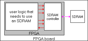
The first three signals on the left are used by the writing agent ("write request", followed by "write address" and "write data"). Then come the three signals for the reading agent. On the right, the controller drives the SDRAM signals. To put things in perspective, here's a view of a typical FPGA system using our SDRAM controller.
Now our controller makes the SDRAM appear as a dual-port memory. But an SDRAM is really a single-port memory, so our controller has to play a trick. If our controller gets two requests simultaneously, either it has to stall one agent, or record their requests and execute them later. Our controller opts for the first strategy. So we added "grant" signals: an agent can assert a request at any time but the controller has the authority to grant the request or not. If a request is denied, keep asking, it will be granted eventually.
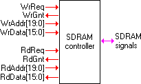
One last complication with SDRAMs comes from the fact that the data returned from read requests is delayed (called the CAS latency in SDRAM datasheets). The controller might also add a few clocks of latency. So even though the controller might grant a read request right away, the matching data is available only a fixed number of clocks later. For convenience, we added a "data valid" signal that is asserted when data is really available.
State machine
Our SDRAM controller's heart is a state machine. The controller waits for a request (read or write), opens the matching bank/row, issue read or write commands (for as long as the active agent requests them in the active row), and finally closes the row.
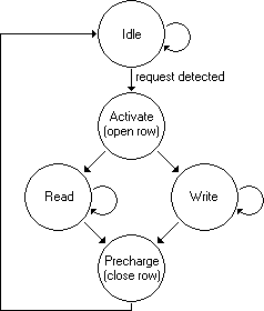
With this scheme, there is only one bank active at a time. Advanced SDRAM controllers would allow multiples banks active simultaneously, but we decided to keep things simple.
Now, opening and closing rows takes time. For example, our SDRAM datasheet provides these numbers:
- tRCD = 20ns (active to read/write)
- tRP = 21ns (precharge to active)
Also refresh cycles are needed if the read agent cannot guarantee opening each row regularly.
The state machine now looks a bit more complicated.
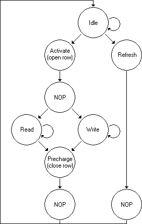
Finally, the number of NOP cycles may need to be adjusted. For example, at 100MHz and with tRP = 21ns, we actually need two NOP cycles after precharge (gives us 30ns before the next activate).
Initialization
The SDRAM has some programmable settings (like the CAS latency), so there is a "MODE" register that needs to be initialized after power-up. A "LOAD MODE" command is used for that purpose. The SDRAM initialization could be added in the controller, or in a separate step before the controller is run.
The code
The heart of our controller is shown below.
To get the best possible IO timing, all the SDRAM control signals are registered so that there is no combinatorial logic signal going outside the FPGA.
always @(posedge clk)  // state machine
case(state)
    2'h0: begin
    	if(RdReq | WrReq) begin  // is there a read or write request?
    		SDRAM_CMD <= SDRAM_CMD_ACTIVE;  // if so, open
    		SDRAM_BA <= Addr[19];  // this bank
    		SDRAM_A <= Addr[18:8];  // this row
    		SDRAM_DQM <= 2'b11;
    		state <= 2'h1;
    	end
    	else
    	begin
    		SDRAM_CMD <= SDRAM_CMD_NOP;  // otherwise stay idle
    		SDRAM_BA <= 0;
    		SDRAM_A <= 0;
    		SDRAM_DQM <= 2'b11;
    		state <= 2'h0;
    	end
    end
    2'h1: begin
    	SDRAM_CMD <= ReadSelected ? SDRAM_CMD_READ : SDRAM_CMD_WRITE;
    	SDRAM_BA <= AddrR[19];
    	SDRAM_A[9:0] <= {2'b00, AddrR[7:0]};  // column
    	SDRAM_A[10] <= 1'b0;  // no auto-precharge
    	SDRAM_DQM <= 2'b00;
    	state <= MoreRequestsInSameBankAndRow ? 2'h1 : 2'h2;
    end
    2'h2: begin
    	SDRAM_CMD <= SDRAM_CMD_PRECHARGE;  // close the row when we're done with it
    	SDRAM_BA <= 0;
    	SDRAM_A <= 11'b100_0000_0000;  // all banks precharge
    	SDRAM_DQM <= 2'b11;
    	state <= 2'h0;
    end
endcase
The complete demo code is available here. It is functional but since this is educational, we kept it as simple as possible by removing non-essential features. Check the comments in the code for the limitations and requirements.
Example of use
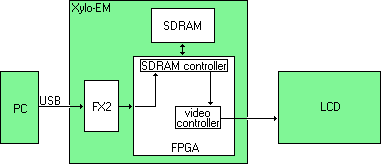
An SDRAM is often used in video cards, as lots of memory is required to store the graphics. It works like that: the computer's CPU sends the graphic data to the video card. The card uses an SDRAM to store the data, and a controller in the card reads periodically the memory to send the data to the display. The data (in the SDRAM) is refreshed automatically in the process.
We created such basic system using a Xylo-EM board as part of our validation process. The fact that the SDRAM controller is dual-ported makes the design straightforward (the PC/FX2 is the writing agent, and the video controller is the reading agent).