

Hardware interface
Spoc memory model
Spoc0 data memory space is 64Kbit deep.- Addresses from 0x0000 to 0x0FFF are reserved for internal use.
- Addresses from 0x1000 to 0xFFFF are free to use by external peripherals. Let's see how to use that!
Writing to peripherals
Write transactions can be 1, 8, 16 or 32 bits wide.
For example:do #0x1000 -> WA0 do.byte #0x55 -> @ // write the 8-bit value 0x55 to the peripheral residing at address 0x1000
Spoc0 has 3 output ports to write to peripherals.
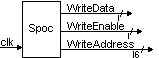
The address port is 16-bit wide (to cover a 64K space) but the data port is only one 1-bit wide (write transactions that are 8, 16 or 32-bit wide require a matching number of clock cycles).
Writing to a 1-bit peripheral
Let's say you require a flag in your FPGA, and the flag needs to be writable by Spoc.
Here we use address 0x3000 for the location of the flag.
reg mySpocFlag;

always @(posedge clk)
begin
	if(WriteEnable & WriteAddress==0x3000) mySpocFlag <= WriteData;
end
A simple routine to write '1' to the flag would be:
do #0x3000 -> WA0
do.bit #1 -> @         // write 1 to the flag
Writing to a n-bits peripheral
... coming soon ...Reading from a peripheral
Reading works similarly to writing, with one big difference. Reading requires a 2-clocks latency from the time the address is provided to the time the data is read by Spoc. This allows "pipelining" the read data-path. This was done because otherwise long data-paths (non-pipelined) can reduce the registered performance (clock speed) of the Spoc design.
For example, let's map the 8-bit value 0x55 at address 0x1000, and 0xAA at address 0x2000.
wire [7:0] MyValue1 = 8'h55;
wire [7:0] MyValue2 = 8'hAA;

// we need 2 registers to create 2 levels of clock latency
reg spoc_ReadData, spoc_ReadData_reg;

always @(posedge clk)   //  one level of clock latency
case(spoc_ReadAddress[15:12])    // coarse address decoding
    4'h1: spoc_ReadData_reg <= MyValue1[spoc_ReadAddress[2:0]];
    4'h2: spoc_ReadData_reg <= MyValue2[spoc_ReadAddress[2:0]];
    default: spoc_ReadData_reg <= 1'b0;
endcase

// second level of clock latency
always @(posedge clk) spoc_ReadData <= spoc_ReadData_reg;
The values are fixed here but could also be any register in the FPGA, or pins (i.e. Spoc could read some FPGA pins).A simple routine to read these values would be:
do #0x1000 -> RA0
do.byte @ -> A        // read 0x55 into accumulator

do #0x2000 -> RA0
do.byte @ -> A        // read 0xAA into accumulator