

PCI Express 4 - The transaction layer
In the transaction layer, we receive "packets". There is a 32-bit bus and the packets arrive on the bus (packet lengths are always multiples of 32 bits). Maybe one packet will says "write data 0x1234 at address 0xABCD", and another will say "read from address 0xDCBA (and return a response packet)".
There are many types of packets: memory read, memory write, I/O read, I/O write, message, completion, etc... Our job in the transaction layer is to accept packets and issue packets. The packets are presented to us in a specific format called "transaction layer packets" (TLPs), and each 32-bit data arriving on the bus is called a "double word" (or DW in short).
So a packet (oops sorry, a TLP) is a bunch of DWs.
How a TLP looks
TLPs are pretty simple to interpret. Here's a general view of their structure.
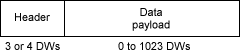
The header contains 3 or 4 DWs but the most important fields are part of the first DW.
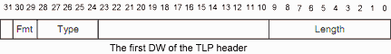
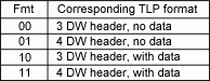
The "Fmt" field tells how long is the header, and if a data payload is present.
Then together with "Type", it describes the TLP operation. The remainder of the TLP header content depends of the TLP operation.
For example, here's a 32-bit memory write TLP header, where you can see that the write address is at the end of the header (and the data to write is in the payload after the header).

The "Fmt" field is "10" which means "3 DW, with data". That makes sense, a memory write needs data to write, so upon getting the data payload after the header, we write that data to some memory (or use it somehow) and we are done with it. The field "Length" tells how many DWs are in the payload (from 0 to 1023). Commonly, it's a single DW to write, in which case length is equal to 1 and the total TLP length is 4 DWs (3 for the header and 1 of the payload).
Now what about a memory read? Somehow we have to return data.
Completion with data
If the TLP is a memory read instead of a write, we have to execute the read and then respond. There is a special TLP for that response, it is called CplD (completion with data) and its payload contains the data that we want to return.
Let's take a closer look at the 32-bit memory read TLP header - it is very similar to the 32-bit memory write we had previously.
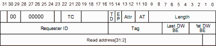
One difference is the Fmt=00, which means "no data". Makes sense, we don't need data to do a read, just an address. But we now have to respond with data. And as important, the response will need to be routed back to whoever asked for the read... Do you see the problem?
Ok, we received a read request. Did it come from the CPU? Or from the interrupt controller? Or from a graphic card? After all, many devices are capable of issuing such request. The answer is given in the "Requester ID" - it shows who requested the read. So when we create the CplD TLP, we have to recopy the "Requester ID" in it. This way, it'll be routed where it belongs by the PCI Express bridge(s). BTW, we also have to recopy the "Tag" (which is useful in case of multiple reads pending).
TLP size
A typical 32-bit address/data memory read TLP is made of 3 DWs in the header and no payload (so 96 bits total), while a similar memory write is made of 4 DWs (3 for the header and 1 for the payload). That's not very efficient in term of bandwidth because of the TLP header overhead, so it is better to use bigger TLP payloads when possible. A TLP payload can theoretically be as big as 1023 DWs, pretty handy for burst reads and writes, although PCs can limit the maximum size to a lower value (32 DWs is typical).
Enough with theory, let's have some fun and play with the Xilinx PCI Express wizard.
Links
- Get the official PCI Express specification by googling something like PCI_Express_Base_20.pdf
- More details on TLPs in How PCI express devices talk