

EPP 3 - The hardware protocol
Here's a view of the DB25 printer connector coming from your PC.
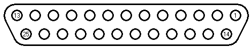
The pins 2 to 9 are the 8-bit bus. In EPP mode, the 8-bit bus is bi-directional.
There other important pins are:
| Pins | Name | Direction | Active | Use |
|---|---|---|---|---|
| 17 | address strobe | PC -> FPGA | low | address transaction |
| 14 | data strobe | PC -> FPGA | low | data transaction |
| 11 | wait | FPGA -> PC | low | response to strobe |
| 1 | write | PC -> FPGA | low | 0 for write transactions, 1 for read transactions |
You can see that there are 2 "strobe" signals plus a "wait" signal. The "strobes" are coming from the PC, while the "wait" is going to the PC.
Here's how this works: for every transaction, the PC asserts one of the strobe and the FPGA responds with the wait.
Let's pick one strobe signal (only one is activated at a time) and let's look at an EPP transaction:
Explanation:
- The PC wants to start a transaction. It asserts one of the strobes (=low).
If the transaction is a write, the PC also drives "write" low, and drives the 8-bit bus.
Otherwise it drives "write" high and leaves the 8-bit bus floating. - The FPGA detects that one of the strobe is asserted, and responds by de-asserting "wait" (=high).
If the transaction is a read, the FPGA starts driving the 8-bit bus. - The PC detects that wait is de-asserted, so it de-asserts the strobe.
If the transaction is a write, the PC stops driving the 8-bit bus. - The FPGA detects that the strobe is de-asserted, so it asserts "wait".
If the transaction is a read, the FPGA stops driving the 8-bit bus.
All this is done in hardware; the PC software doesn't have to do anything besides starting the transaction.