

Direct Digital Synthesis 2 - Arbitrary signals
To generate arbitrary signals, DDSs rely on two main tricks.
LUT
The first DDS trick is a LUT (lookup table). The LUT is a table that holds the shape of the analog signal we want to generate.
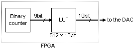
In an FPGA, the LUT is implemented as blockrams. In the picture above, we used a 512x10bit LUT, which usually fits into one or two physical FPGA blockrams.
Sine wave
The most commonly generated signal shape is a sine wave. It is particular as it has two symmetries that can be easily exploited to make the LUT appear bigger.
In a sine wave, the first symmetry is sin(α)=sin(π-α).
Assuming our "my_DDS_LUT" blockram is instantiated like that
wire [9:0] LUT_output;

blockram512x10bit_2clklatency my_DDS_LUT(.rdclock(clk), .rdaddress(cnt[8:0]), .q(LUT_output));
we simply have to access the LUT in the reverse the direction after a half-period to exploit the first symmetry.
blockram512x10bit_2clklatency my_DDS_LUT(.rdclock(clk), .rdaddress(cnt[9] ? ~cnt[8:0] : cnt[8:0]), .q(LUT_output));
So now we store only half of the wave in the blockram, but its content is used twice for each period of the output signal. In a sense, the LUT appears as a 1024x10bit (and using the second symmetry, we get a 2048x10bit).
Note that we use a blockram "blockram512x10bit_2clklatency" that provides data with two clocks latency (because one clock latency blockrams are slower). How this is done is FPGA vendor dependent (Altera would use LPMs while Xilinx would use primitives).
Let's rewrite the LUT as a separate module that exploits the two sine symmetries.
// sine lookup value module using two symmetries
// appears like a 2048x10bit LUT even if it uses a 512x10bit internally
// 3 clock latency
module sine_lookup(input clk, input [10:0] addr, output reg [16:0] value);

wire [15:0] sine_1sym;  // sine with 1 symmetry
blockram512x16bit_2clklatency my_quarter_sine_LUT(     // the LUT contains only one quarter of the sine wave
    .rdclock(clk),
    .rdaddress(addr[9] ? ~addr[8:0] : addr[8:0]),   // first symmetry
    .q(sine_1sym)
);

// now for the second symmetry, we need to use addr[10]
// but since our blockram has 2 clock latencies on reads
// we need a two-clock delayed version of addr[10]
reg addr10_delay1; always @(posedge clk) addr10_delay1 <= addr[10];
reg addr10_delay2; always @(posedge clk) addr10_delay2 <= addr10_delay1;

wire [15:0] sine_2sym = addr10_delay2 ? {1'b0,-sine_1sym} : {1'b1,sine_1sym};  // second symmetry

// add a third latency to the module output for best performance
always @(posedge clk) value <= sine_2sym;
endmodule
Note that the sine_lookup module has a total of 3 clock latencies (two from the blockram, and one from the registered output at the end).
Having clock latencies has the benefit of pipelining the operation and getting the maximum possible performance out of the FPGA.
Don't forget that this needs to run at at least 100MHz.
Also we increased the output width of our blockram from 10bit to 16bit (the 6 extra bits are lost if unused in our particular FPGA blockram, so we might as well implement them). We'll put the extra bits in good use in part 4.
To effectively use our newly made "sine_lookup module", we can simply write
reg [10:0] cnt;
always @(posedge clk) cnt <= cnt + 11'h1;

wire [16:0] sine_lookup_output;
sine_lookup my_sine(.clk(clk), .addr(cnt), .value(sine_lookup_output));

wire [9:0] DAC_data = sine_lookup_output[16:7];   // for now, we drop the LSBs to feed our DAC
                                                  // (since it takes only 10 bits)
and we get a nice sine wave from the DAC.